I am a B.Eng. candidate in Microelectronics Science and Engineering at Central South University, with an expected graduation date of June 2027. My current work lies at the device-circuit interface, spanning semiconductor-device simulation, memristor behavioral and circuit modeling, and the translation of device dynamics into circuit-level operating constraints.
I am seeking PhD opportunities for Fall 2027 to extend this foundation toward device-aware analog, mixed-signal, and power-management ICs for wide-bandgap power conversion. I am especially interested in adaptive GaN/SiC gate-driver ICs and in translating device, package, thermal, and parasitic constraints into circuit specifications for sensing, timing, drive, high-voltage interfacing, protection, and robust validation.
First authorModeling, simulation, analysis, and writing
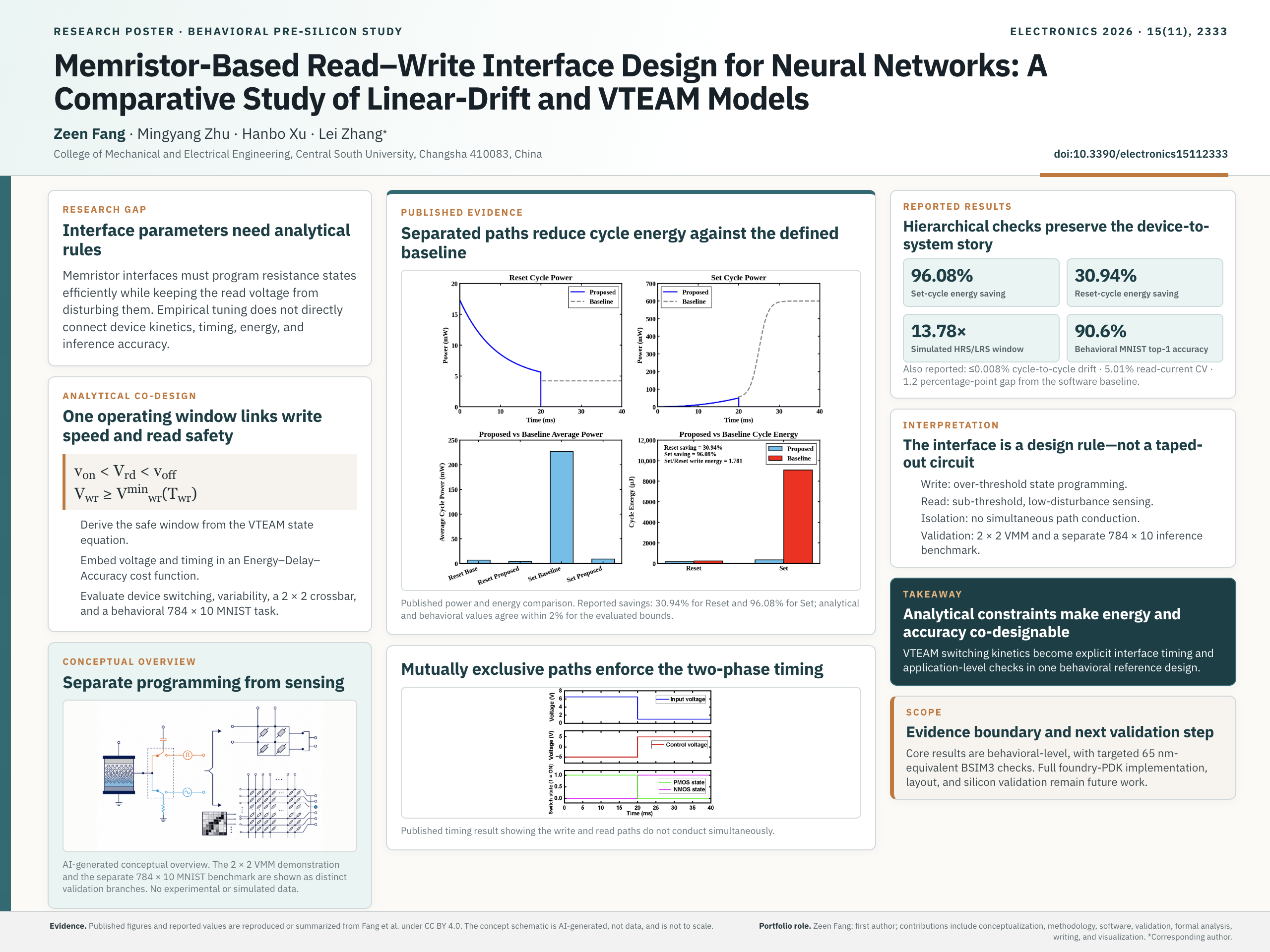
A behavioral-level, pre-silicon study deriving analytical read-write constraints from the VTEAM state equation and evaluating them from device to neural-network scale.
The published study reports a 13.78x resistance window and 90.6% MNIST top-1 accuracy, with 96.08% Set-cycle energy reduction against its defined behavioral baseline.
Third authorValidation, data curation, and manuscript review
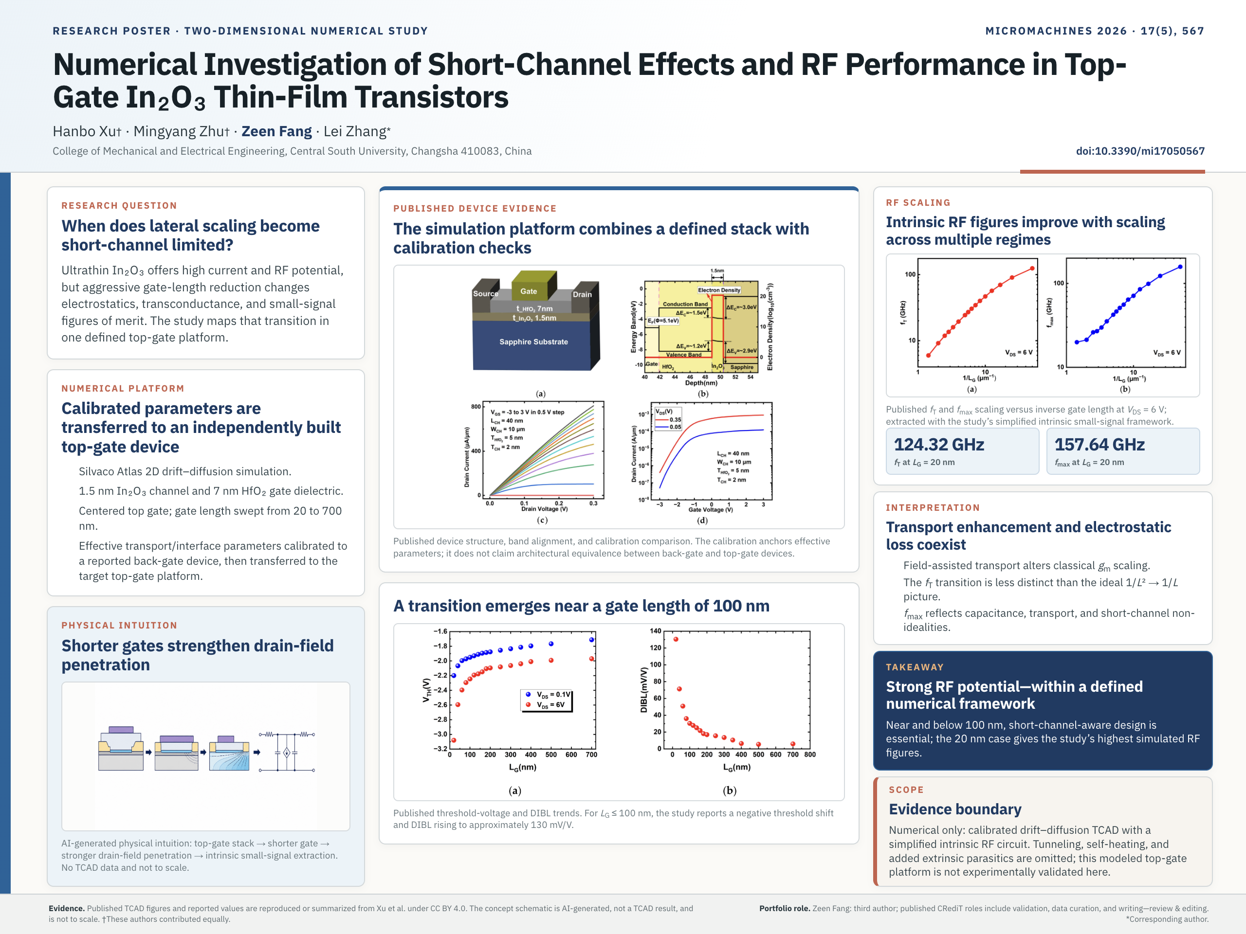
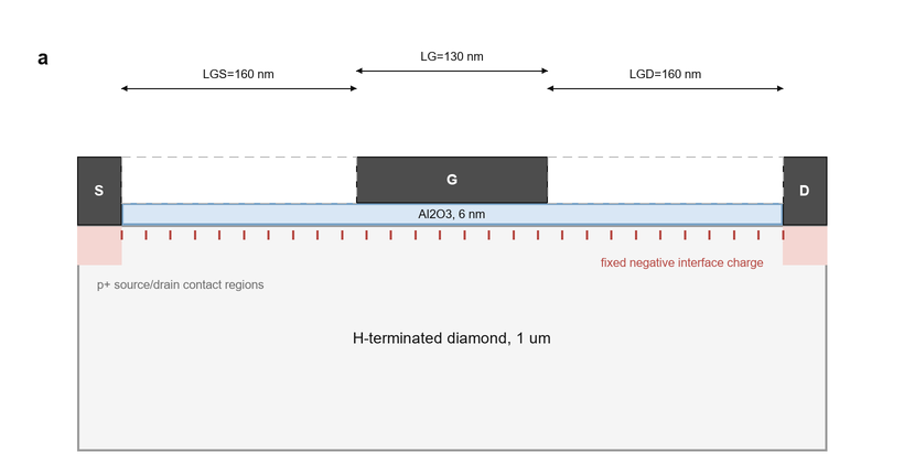
A two-dimensional numerical study of short-channel behavior and simulated DC/RF scaling across 20-700 nm top-gate In₂O₃ TFTs.
My credited roles were validation, data curation, and manuscript review and editing; the highlighted device and RF values are study-level numerical results.
Published work is listed above. Ongoing research and team engineering projects are identified here with their current evidence and status.
A Second-Order Memristor SPICE Model for Neuromorphic Circuit Analysis
Ongoing research · Manuscript in preparation · IEEE TCAS-I target · 2026-present
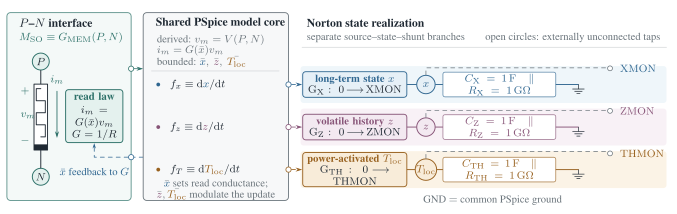
I am developing a PSpice second-order memristor model that separates a retained conductance state from a relaxing history state, with a power-activated auxiliary state. Matched-x paired-pulse, selected 1T1R, STDP-like, and compact 2 × 2 simulations connect internal-state attribution to circuit-level behavior.
Simulation-only: 11.16% matched-x interval sensitivity versus 1.01% for the separately simulated history-off family; STDP-like ΔG = -1.82% to +1.09%; 24 compact-array read cases with no more than 0.450% unit-range state disturbance. The target denotes planned submission style only.
Current PSpice implementation · simulation only
Team LDO competition project — Zengyi Huichuang Cup
10th National College Student IC Innovation and Entrepreneurship Competition · 2026
Team project
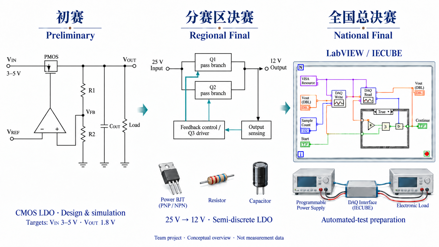
As a team member, I contributed to selected tasks across the competition stages: a 1.8 V CMOS LDO, eight simulation benches, a physical-verification trail, regional semi-discrete hardware, and national-stage automated-test preparation.
AI-generated conceptual overview, not the team's implementation schematic or measurement data. The LabVIEW interface illustrates national-final test preparation, not a completed or executable test system.
Selected team contributions under instructor guidance. CMOS work covers design and simulation; regional hardware is a separate semi-discrete LDO; automated testing remained preparation.
Design stages & original technical evidence
01
Team design & simulation
1.8 V CMOS LDO
SMIC 180 nm transistor-level work covering a PMOS pass device, bandgap reference, folded-cascode error-amplifier path, feedback, bias, and compensation, followed by eight dedicated simulation benches.
02
Physical workflow
Layout-level evaluation
Top-level layout integration, Calibre DRC/LVS/PEX, and post-layout simulation. The detailed case file keeps the unresolved DRC results and line-regulation gap visible.
03
Team hardware task
Regional-final LDO
BJT characterization and selection using TIP42C/TIP32C and BD139/BD135 candidates, followed by a 25 V-to-12 V semi-discrete LDO and regulation, stability, transient, and thermal evaluation.
04
Preparation only
Automated test workflow
IECUBE-3100/3839 and LabVIEW preparation for PWS/DIO/DMM control, voltage-accuracy, line/load-regulation and dropout scans, data logging, and result logic.
I constrained a Codex harness around local Silvaco ATLAS to turn paper reading, parameterized device sweeps, log parsing, figure generation, and scientific stop rules into one traceable research-training loop.
Codex supported workspace inspection, experiment matrices, parsing, and audits; ATLAS remained the solver, while I owned the physical assumptions, run authorization, stopping rules, and claim promotion.
My intended PhD direction is device-aware analog and mixed-signal IC design for wide-bandgap power conversion. I want to translate nonlinear device behavior, parasitics, temperature, and package effects into on-chip sensing, timing, drive, high-voltage interface, and protection decisions.
Candidate doctoral blocks
ObserveGate/current sensingLow-latency state extraction with limited loading and bounded sensitivity to PVT and switching noise.
InterfaceTiming and high-voltage interfacesReference and delay generation, high-CMTI level shifting, and bootstrap or floating-supply interfaces.
Act & protectAdaptive drive and protectionSegmented predrivers and output stages, dead-time or drive control, and fast protection for GaN/SiC power stages.
Device-to-specification translationPublished In₂O₃ numerical studyInterpreting device assumptions, scaling behavior, capacitance, and parasitic trends as circuit-design constraints.
IC workflow exposureTeam LDO competition projectSelected team tasks spanning schematic analysis, physical verification, post-layout evaluation, and semi-discrete hardware testing.
Verification milestones
Progressive verification path
Proposed and resource-dependent
01Baseline gate
Reproduce a representative circuit and freeze one focused specification.
02Robustness gate
Evaluate PVT, mismatch, parasitics, reliability, CMTI, and testability.
03Implementation gate
Advance through transistor-level design, layout, DRC/LVS/PEX, and post-layout verification.
04Hardware gate
Proceed to prototype, tapeout, or measurement only when resources and earlier evidence permit.
These are candidate entry points, not completed designs or a thesis solution fixed in advance. I expect to begin with one well-grounded power-IC block, selected after baseline reproduction and assessment of available project and fabrication resources.
Education & Preparation
Central South University
2023.09-2027.06 (expected)
B.Eng. Candidate in Microelectronics Science and Engineering
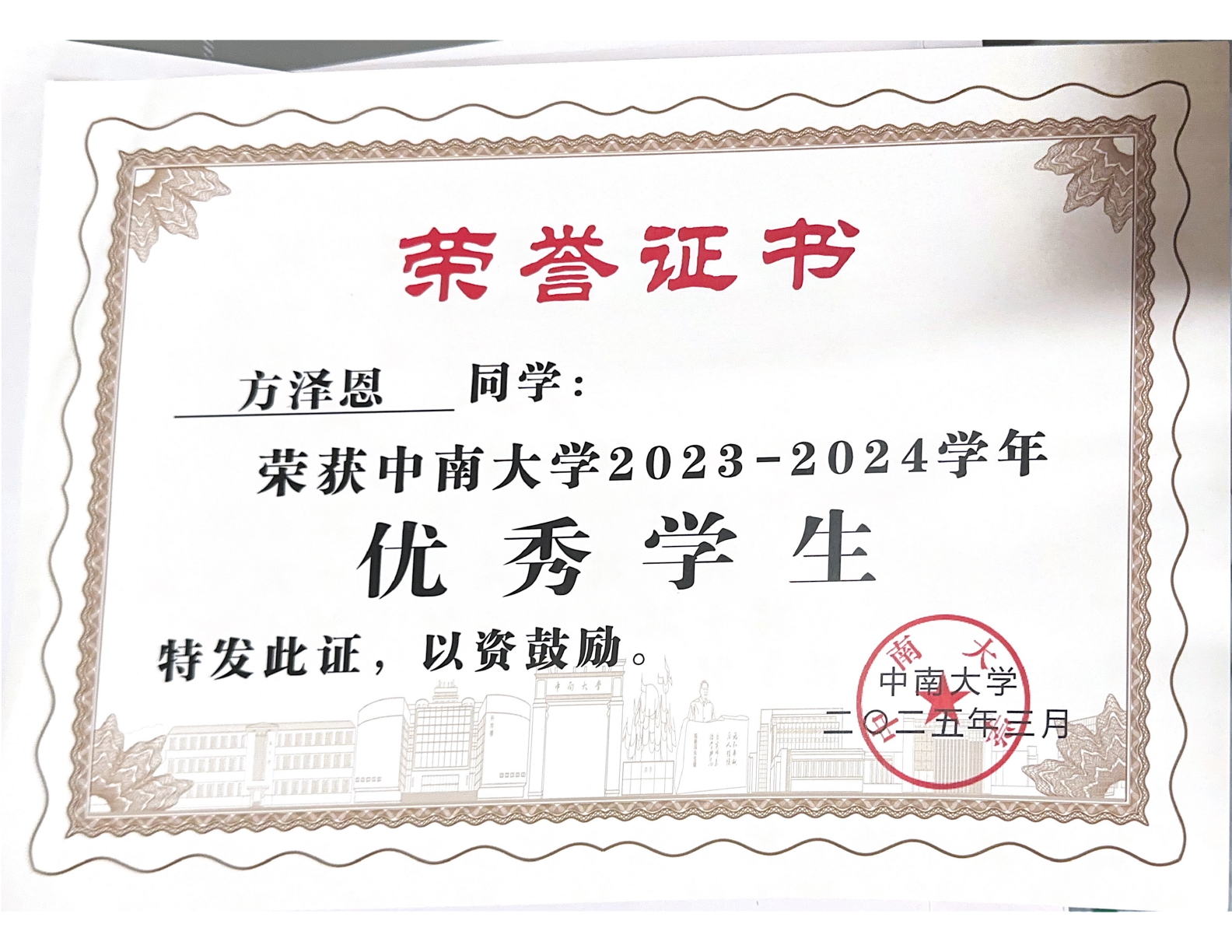
Outstanding Student · Central South University, 2023–2024
Selected coursework: Semiconductor Device Physics, Circuit Theory, Analog and Digital Electronic Technology, Signals and Systems, and Large-Scale Integrated Circuit Design.
Modeling & simulation
Semiconductor-device simulation, behavioral circuit modeling, MATLAB, and PSpice.
Full honours list · competitions, scholarships & student awards
Second Prize, National Final; First Prize, Central China Regional Final — 10th National College Student IC Innovation and Entrepreneurship Competition, Zengyi Huichuang Track · team award
Second Prize, Hunan Division; Excellence Award, National Final — 28th China Robot and Artificial Intelligence Competition, Humanoid Sprint · team awards
Honorable Mention, Mathematical Contest in Modeling · team award
Outstanding Student, College of Mechanical and Electrical Engineering, Central South University · certificate issued March 2026
Third Prize, Central South University Mathematics Competition · Non-Mathematics Category
First Prize, Hunan Division, 16th Chinese Mathematics Competition for College Students · Non-Mathematics Category A
First Prize, 8th Hunan Provincial College Students Mathematics Competition · Non-Mathematics Category A
Excellent Student Award, Highpower International Scholarship
Outstanding Student, Central South University
Second-Class Academic-Year Scholarship, Central South University
Fall 2027 PhD applications
Open to doctoral research conversations.
I am preparing applications to PhD programs in microelectronics, electrical and computer engineering, and related fields. If my device-to-circuit background aligns with your group's research, I would be glad to discuss potential doctoral directions.