曾益慧创杯 · Team LDO project · 2026
From schematic to post-layout evaluation
A 1.8 V CMOS LDO team project in SMIC 180 nm. My work included selected schematic analysis, PVT/PSRR/STB simulation, layout and Calibre practice, post-layout evaluation, and regional hardware tasks.
- ≈126 mV
- reported dropout
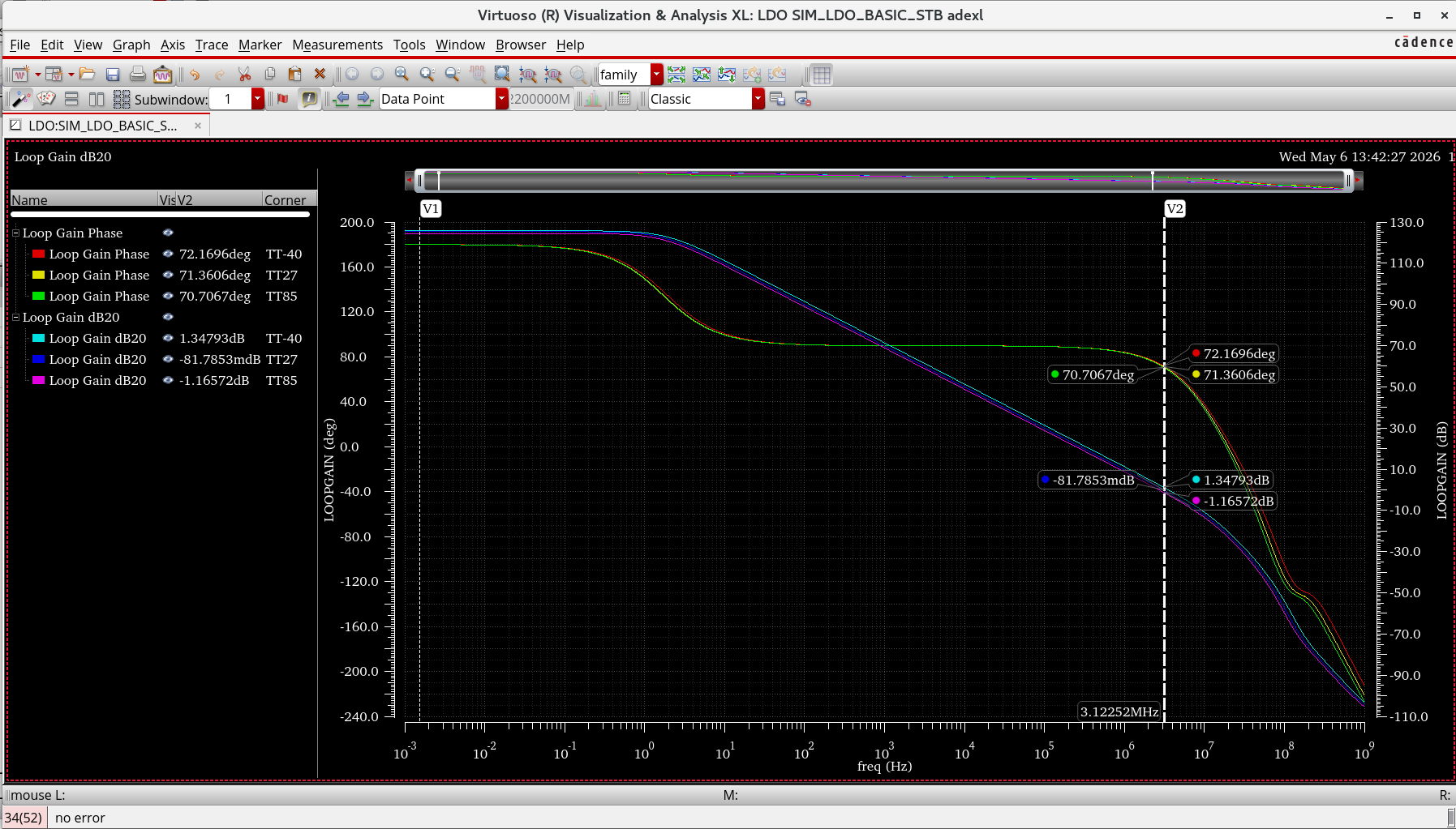
- 67.9-74.5°
- post-layout phase margin
- 65.9-69.3 dB
- PSRR at 1 kHz
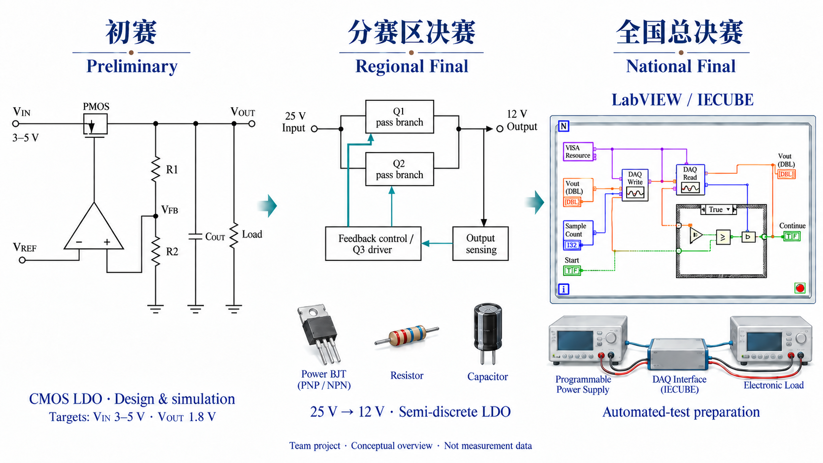
AI-generated conceptual overview, not the team's implementation schematic or measurement data. The LabVIEW interface illustrates national-final test preparation, not a completed or executable test system.
Four connected tasks
- 01
Team design & simulation
1.8 V CMOS LDO
Architecture review and eight dedicated simulation benches in SMIC 180 nm. - 02
Physical workflow
Layout, LVS, PEX, post-layout
Layout, LVS, parasitic extraction, and post-layout evaluation. - 03
Team hardware task
Regional semi-discrete LDO
A separate 25 V-to-12 V BJT regulator built and debugged at the regional final. - 04
Preparation record
National-stage automated testing
LabVIEW/IECUBE preparation for instrument control, scans, logging, and safe recovery.
1.8 V CMOS LDO architecture
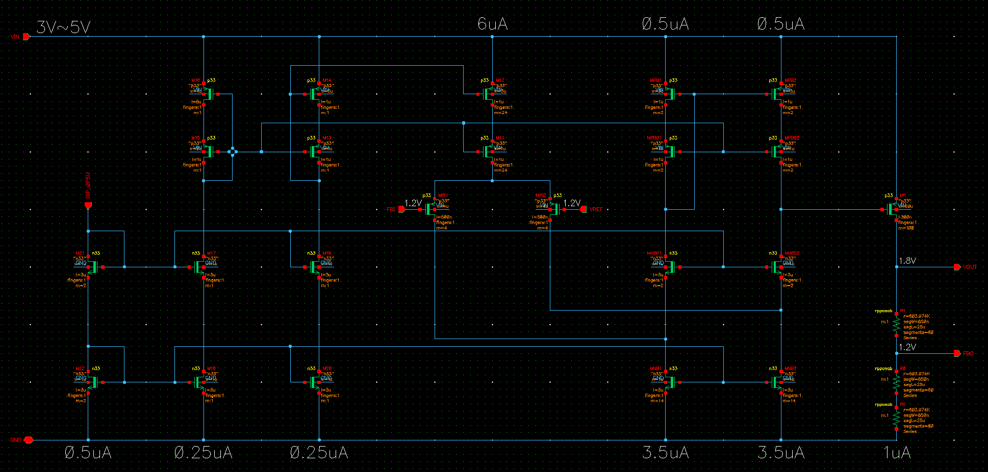
The team design targets a 1.8 V output from a 3-5 V supply in a 0.18 µm CMOS process. A bandgap-derived reference, feedback network, error amplifier, bias network, common-source driver, and PMOS pass device close the regulation loop around a 1 µF external output capacitor. The error amplifier uses a PMOS-input folded-cascode first stage followed by a common-source stage.
- ReferenceBandgap core
≈1.2 V reference
- Error sensingPMOS-input folded cascode
Compares feedback with the reference
- Gate driveCommon-source stage
Drives the large PMOS gate
- Power pathPMOS pass device
Regulates current from VIN to VOUT
- FeedbackResistor network
Returns a scaled VOUT to the amplifier
- Process
- 0.18 µm CMOS
- Operating envelope
- VIN 3-5 V · VOUT 1.8 V
- Temperature
- -40 / 27 / 85 °C
- Core checks
- DC · regulation · Iq
SMIC design environment
1 µF external output capacitor
TT, FF, SS, FS, and SF report labels
PSRR · dropout · stability
Eight dedicated testbenches
Separate ADE environments cover operating point, accuracy, line/load regulation, dropout, quiescent current, PSRR, and loop stability. The report uses TT/FF/SS/FS/SF labels; some archived state names still need mapping before a clean rerun.
- 01
SIM_LDO_BASIC_DCOperating point and transistor headroom
- 02
SIM_LDO_ACCURACYOutput error under the declared point set
- 03
SIM_LDO_LINEARVIN sweep and line-regulation extraction
- 04
SIM_LDO_LOADINGLoad sweep and load-regulation extraction
- 05
SIM_LDO_DROPOUTVIN threshold search against the output limit
- 06
SIM_LDO_CURRENTQuiescent-current evaluation
- 07
SIM_LDO_PSRRSupply-ripple rejection at declared frequencies
- 08
SIM_LDO_STBLoop gain, phase margin, and gain margin
Post-layout results and remaining gaps
| Metric | Reported result | Assessment |
|---|---|---|
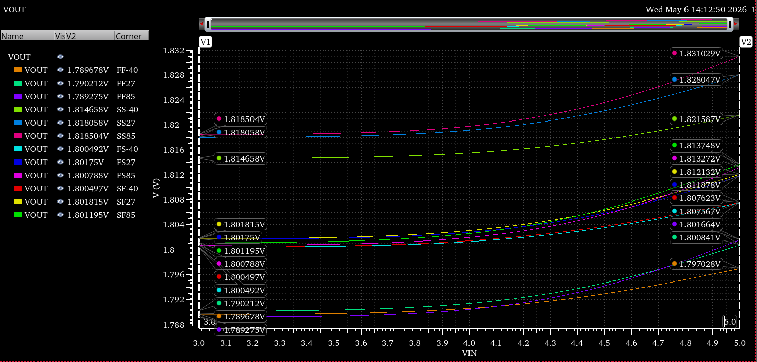
| Output accuracyPartial closure | 1.7893-1.8186 V in the accuracy table; the line sweep reaches about 1.8310 V. | Typical/base point supported; the full-envelope ±1% target is not closed. |
| Load regulationRerun needed | 0.312 mV pre-layout PVT worst case; no recovered post-layout raw point table. | Promising, but a clean post-layout rerun is still needed. |
| Line regulationOpen gap | About 12.5 mV across VIN = 3-5 V at the visible SS/85 °C worst case. | Open gap against the ≤3 mV base target. |
| Quiescent currentBase supported | 8.745-9.173 µA at the reported base-condition load. | Meets the ≤10 µA base target; the advanced condition is not supported. |
| PSRRBase supported | 65.91-69.27 dB at 1 kHz in the post-layout report. | Meets the >60 dB base target; broadband >70 dB is not closed. |
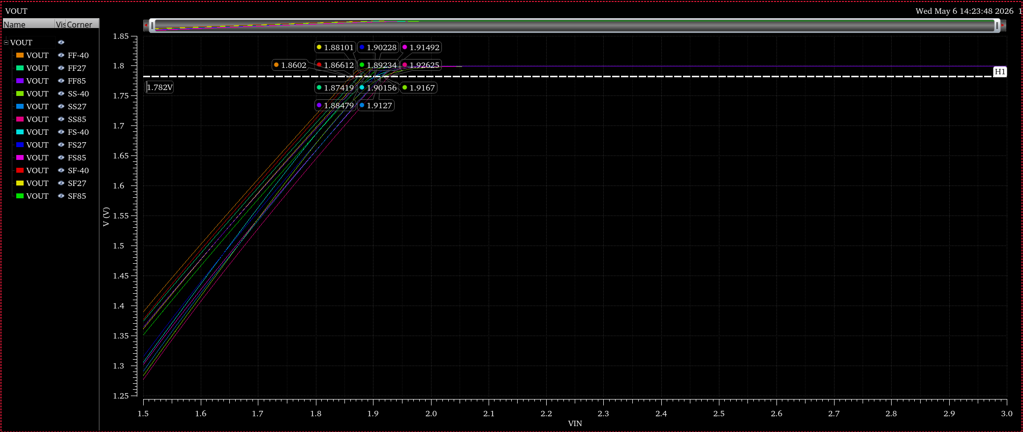
| DropoutReport-backed | Approximately 126 mV in the report; worst marked VIN is near 1.926 V. | Within the ≤200 mV base target; raw PEX outputs are missing. |
| Loop stabilityArchive-supported | 67.92-74.54° phase margin and 21.36-22.35 dB gain margin. | Strong post-layout simulation result; not a silicon measurement. |
Layout and physical verification
Layout
Present
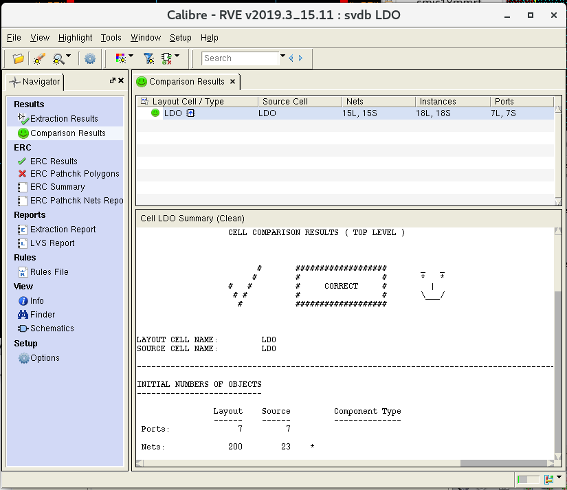
Top-level integration is preserved in the archive.LVS
CORRECT
Recovered comparison shows schematic-layout connectivity agreement.PEX
Generated with warnings
Extraction and post-layout plots are present; warnings remain.DRC
1007 results
1007 results in 8 of 423 checks; not DRC-clean sign-off.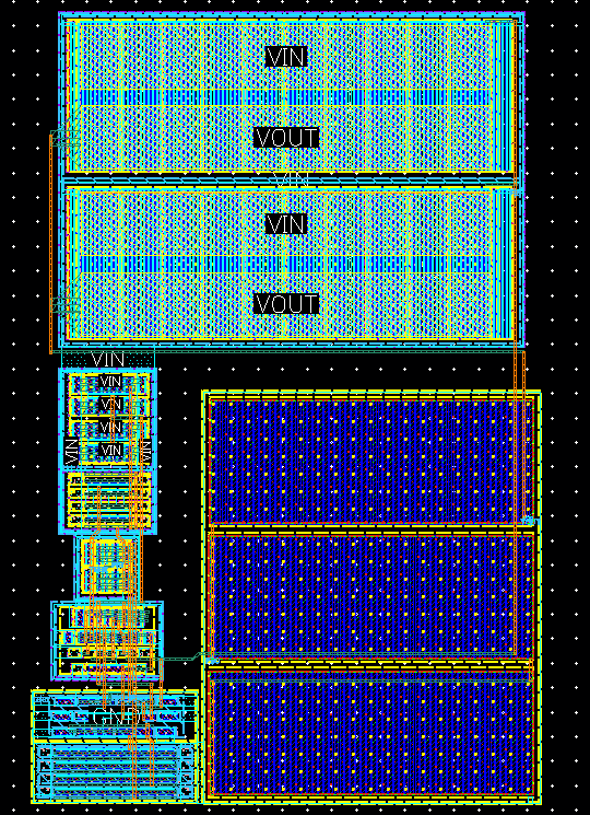
Archive status
Front-end states survive; the post-layout hand-off is incomplete.
- The primary archive retains the design library, ADE/Spectre states, and eight named testbenches.
- The nested submission archive is truncated.
- Plots survive, but the extracted netlist and full raw result database do not.
25 V-to-12 V semi-discrete regulator
The regional final was a separate hardware task: BJT characterization, component selection, assembly, and debugging of a semi-discrete feedback regulator. It was not post-silicon testing of the CMOS LDO.
- 01
Characterize TIP42C/TIP32C and BD139/BD135 candidate BJTs
- 02
Select and match devices; calculate feedback and compensation values
- 03
Assemble and debug a 25 V-to-12 V semi-discrete feedback LDO
- 04
Evaluate regulation, dropout, stability, load transient, and thermal behavior
Automated-test preparation
For the national stage, I prepared a LabVIEW/IECUBE test architecture for PWS, DIO, DMM, and waveform resources. The design separates DUT settings from the interface and keeps a safe shutdown path for success, abort, and error.
- 01Initialize safely
Open sessions, validate limits, and keep all outputs disabled.
- 02Set the operating point
Apply VIN and load through a configurable DUT map.
- 03Measure
Acquire actual voltage, current, and waveform data after settling.
- 04Calculate and save
Store raw points, worst cases, units, limits, and validity together.
- 05Shut down
Return the load to safety, turn VIN off, discharge, and close sessions.
Keep every raw sweep point, calculate the worst valid case, and return results below the instrument floor as invalid or indeterminate—not as passes. The archived work is preparation, not a completed hardware PASS/FAIL dataset.
How I present this project
This project shows selected contributions within a team analog-IC workflow: circuit reading, simulation, layout/Calibre practice, post-layout analysis, regional hardware debugging, and test-system preparation.
It does not claim independent LDO ownership, DRC-clean sign-off, tapeout, fabrication, post-silicon validation, a complete PEX rerun package, or a finished LabVIEW hardware-validation system.